AstraControl

ESP32-based control PCB uses WiFi with an external antenna and 5Mbps RS-485 for communication, supporting various sensors and HMI devices for high-power LED fixtures or strips. Device can be configured to be a master or slave. The board connects to AstraDriver a high power LED driver board that uses 4x LED2001 drivers. Direct copper heat-sink PCB for LED diode AstraBeamLED. Power Distribution board AstraControlPower.
Table of contents
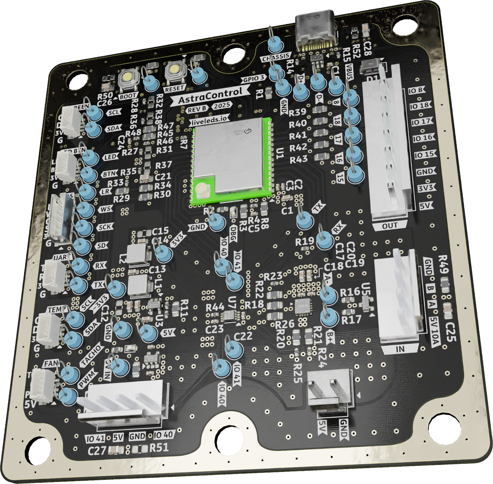
Render Top Angled

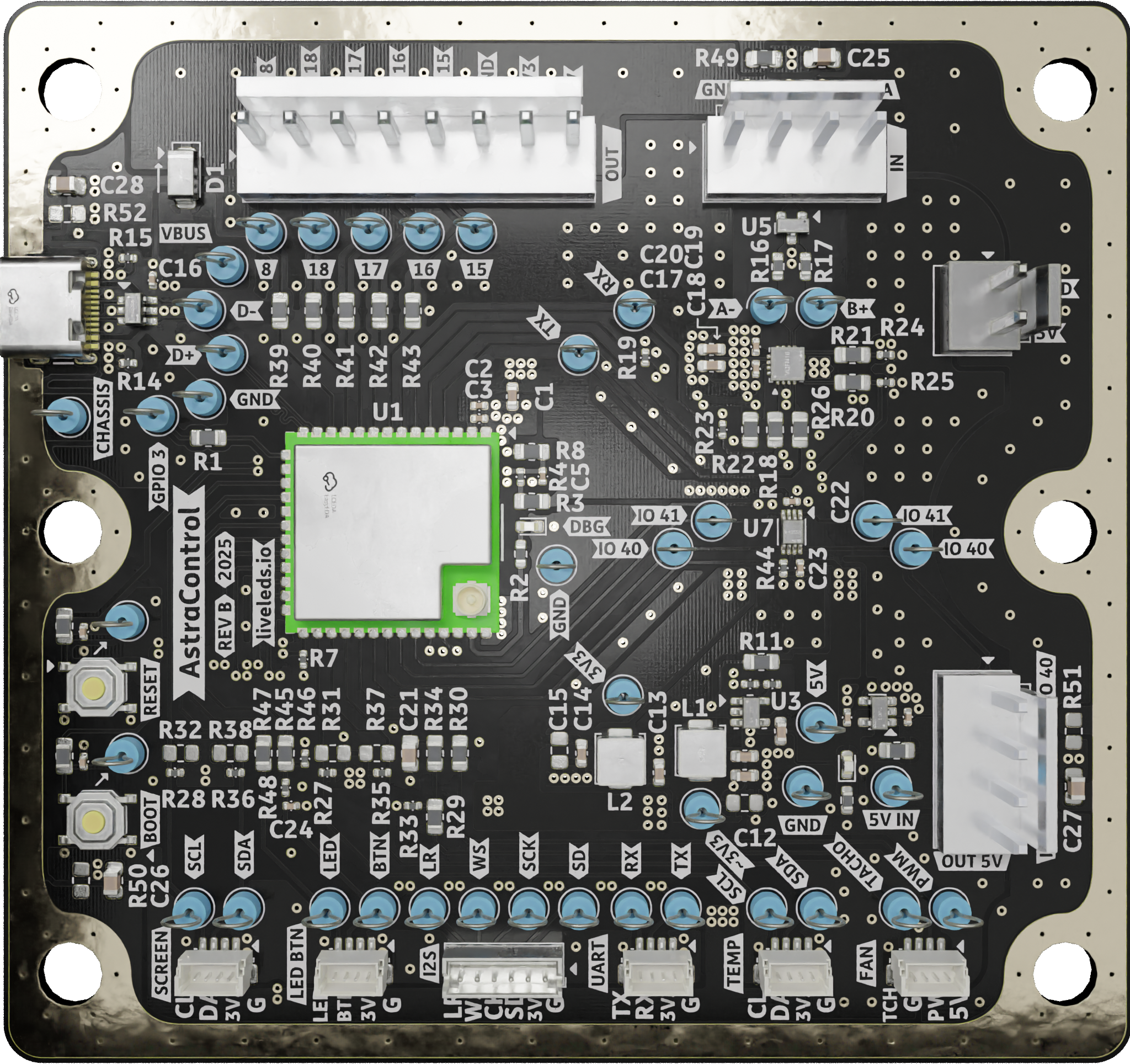
Render Top

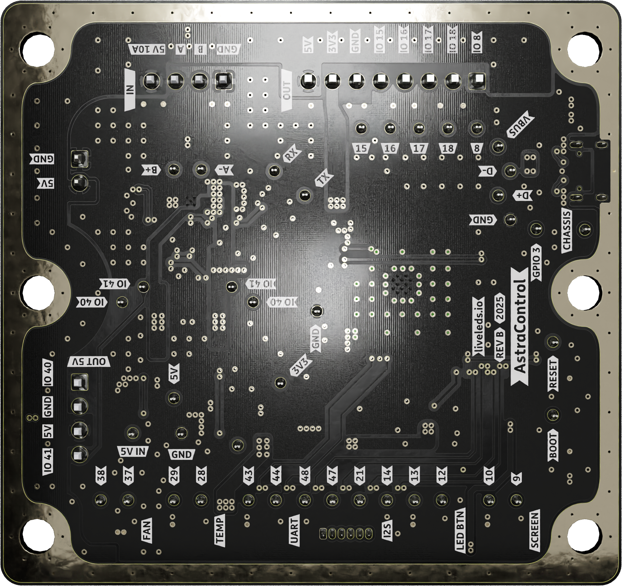
Render Bottom

Schematic
Dark
Monochromatic
Light
Assembly
Dark
Light
Gerber viewer on tracespace.io
Interactive BOM
Check component locations by hovering over a specific component. The visual elements might not be precise enough for pcb review but can be very useful since it’s possible to pan and zoom. Not all BOM columns are available here, for datasheet links see BOM below.
BOM
All components with Values, References, Sheetpath and Links to the datasheet.
KiCad Revision Inspector (KiRI)
KiCad Revision Inspector (KiRI) is a tool for comparing different versions of KiCad projects. It exports project revisions to SVG format for visual comparison using an onion skin view. This helps identify changes and errors in PCB designs. KiRI also includes a command line interface for generating viewable artifacts in any web browser.
View the PCB / Schematic in an interactive way, pan and zoom to see the details.
Dark
Light
Downloads
JLCPCB
Eurocircuits
3D Step
Report
ERC
ERC Report
- Errors: 0
- Warnings: 0
- Link: HTML Report
DRC
DRC Report
- Errors: 1
- Warnings: 3
- Link: HTML Report
Repository
PCB
Board size: 102.0x96.0 mm (4.02x3.78 inches)
- This is the size of the rectangle that contains the board
- Thickness: 1.61 mm (63 mils)
- Material: FR4
- Finish: ENIG
- Layers: 4
- Copper thickness: 35 / 15 µm
Solder mask: TOP / BOTTOM
- Color: Black
Silk screen: TOP / BOTTOM
- Color: White
Stackup:
Impedance controlled: YES
| Name | Type | Color | Thickness [µm] | Material | Er | Loss tan |
|---|---|---|---|---|---|---|
| F.SilkS | Top Silk Screen | White | ||||
| F.Paste | Top Solder Paste | |||||
| F.Mask | Top Solder Mask | 10 | ||||
| F.Cu | copper | 35 | ||||
| dielectric 1 | prepreg | FR4 natural | 210 | FR4 | 4.4 | 0.020 |
| In1.Cu | copper | 15 | ||||
| dielectric 2 | core | FR4 natural | 1065 | FR4 | 4.6 | 0.020 |
| In2.Cu | copper | 15 | ||||
| dielectric 3 | prepreg | FR4 natural | 210 | FR4 | 4.4 | 0.020 |
| B.Cu | copper | 35 | ||||
| B.Mask | Bottom Solder Mask | 10 | ||||
| B.Paste | Bottom Solder Paste | |||||
| B.SilkS | Bottom Silk Screen | White |
Important sizes
Clearance: 0.2 mm (8 mils)
Track width: 0.19 mm (8 mils)
- By design rules: 0.15 mm (6 mils)
Drill: 0.4 mm (16 mils)
- Vias: 0.5 mm (20 mils) [Design: 0.3 mm (12 mils)]
- Pads: 0.4 mm (16 mils)
- The above values are real drill sizes, they add 0.1 mm (4 mils) to plated holes (PTH)
Via: 0.8/0.4 mm (31/16 mils)
- By design rules: 0.35/0.2 mm (14/8 mils)
- Micro via: yes [0.2/0.1 mm (8/4 mils)]
- Buried/blind via: yes
- Total: 453 (thru: 453 buried/blind: 0 micro: 0)
Outer Annular Ring: 0.05 mm (2 mils)
- By design rules: 0.03 mm (1 mils)
Eurocircuits class: 10C
- Using min drill 0.4 mm for an OAR of 0.05 mm
General stats
Components count: (SMD/THT)
- Top: 99/48 (SMD + THT)
- Bottom: 0/0 (NONE)
Defined tracks:
- 0.24 mm (9 mils)
- 0.3 mm (12 mils)
- 0.35 mm (14 mils)
- 0.5 mm (20 mils)
- 0.9 mm (35 mils)
- 1.0 mm (39 mils)
Used tracks:
- 0.19 mm (8 mils) (18) defined: no
- 0.2 mm (8 mils) (11) defined: no
- 0.24 mm (9 mils) (21) defined: yes
- 0.28 mm (11 mils) (41) defined: no
- 0.3 mm (12 mils) (29) defined: yes
- 0.35 mm (14 mils) (354) defined: yes
- 0.5 mm (20 mils) (54) defined: yes
- 0.54 mm (21 mils) (1) defined: no
- 0.56 mm (22 mils) (17) defined: no
- 0.6 mm (24 mils) (14) defined: no
- 0.8 mm (31 mils) (1) defined: no
- 0.85 mm (33 mils) (2) defined: no
- 0.9 mm (35 mils) (15) defined: yes
- 1.0 mm (39 mils) (3) defined: yes
Defined vias:
- 0.35/0.2 mm (14/8 mils)
- 0.55/0.25 mm (22/10 mils)
- 0.7/0.3 mm (28/12 mils)
- 0.8/0.4 mm (31/16 mils)
Used vias:
- 0.8/0.4 mm (31/16 mils) (Count: 453, Aspect: 2.0 A) defined: yes
Holes (excluding vias):
- 0.3 mm (12 mils) (17)
- 0.4 mm (16 mils) (84)
- 0.6 mm (24 mils) (2)
- 0.73 mm (29 mils) (6)
- 0.9 mm (35 mils) (41)
- 1.8 mm (71 mils) (18)
- 5.8 mm (228 mils) (6)
Oval holes:
- 0.62x1.4 mm (24x55 mils) (2)
- 0.62x1.7 mm (24x67 mils) (2)
Drill tools (including vias and computing adjusts and rounding):
- 0.4 mm (16 mils) (17)
- 0.5 mm (20 mils) (537)
- 0.6 mm (24 mils) (2)
- 0.7 mm (28 mils) (4)
- 0.85 mm (33 mils) (6)
- 1.0 mm (39 mils) (41)
- 1.9 mm (75 mils) (18)
- 5.9 mm (232 mils) (6)
Solder paste stats:
Using a paste with 87.75 % alloy, that has an specific gravity for the alloy of 7.4 g/cm³ and 1.0 g/cm³ for the flux. This paste has an specific gravity of 4.15 g/cm³.
The stencil thickness is 0.12 mm.
| Side | Pads with paste | Area [mm²] | Paste [g] |
|---|---|---|---|
| Total | 317 | 311.33 | 1.55 |
Note: this is just an approximation to the theoretical value. Margins of the solder mask and waste aren’t computed.
Know Issues
- TBD
Credits
Amulet - Inspiration for awesome schematic and PCB
tracespace view - Online Gerber Viewer
