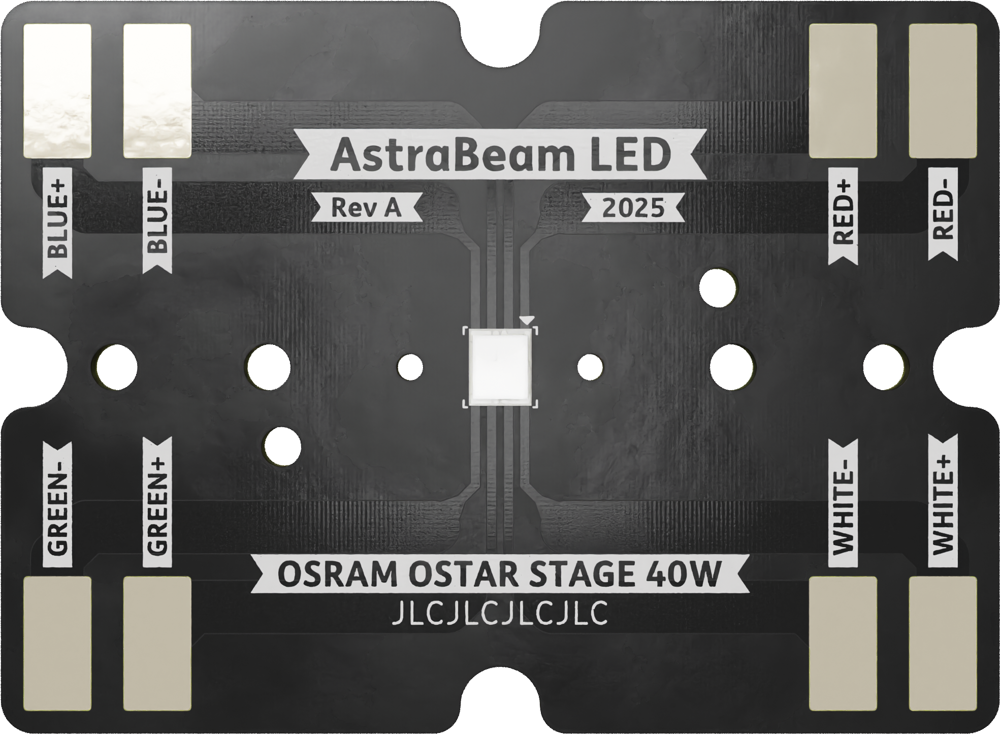
AstraBeamLED
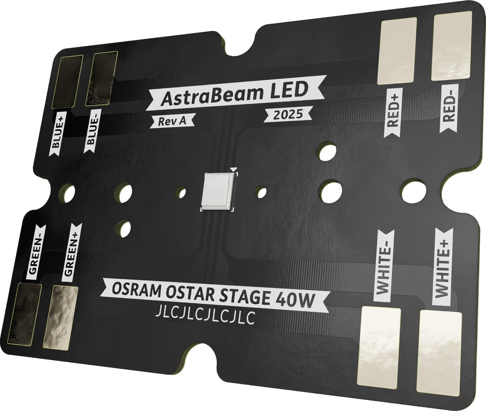
OSRAM OSTAR® Stage Light PCB LE RTDUW S2WN
High Power 40W RGBCY LED PCB with direct heatsink copper base.
Production Details
The PCB went into production on April 9, 2025.
- Git Tag:
production-2025.04.09
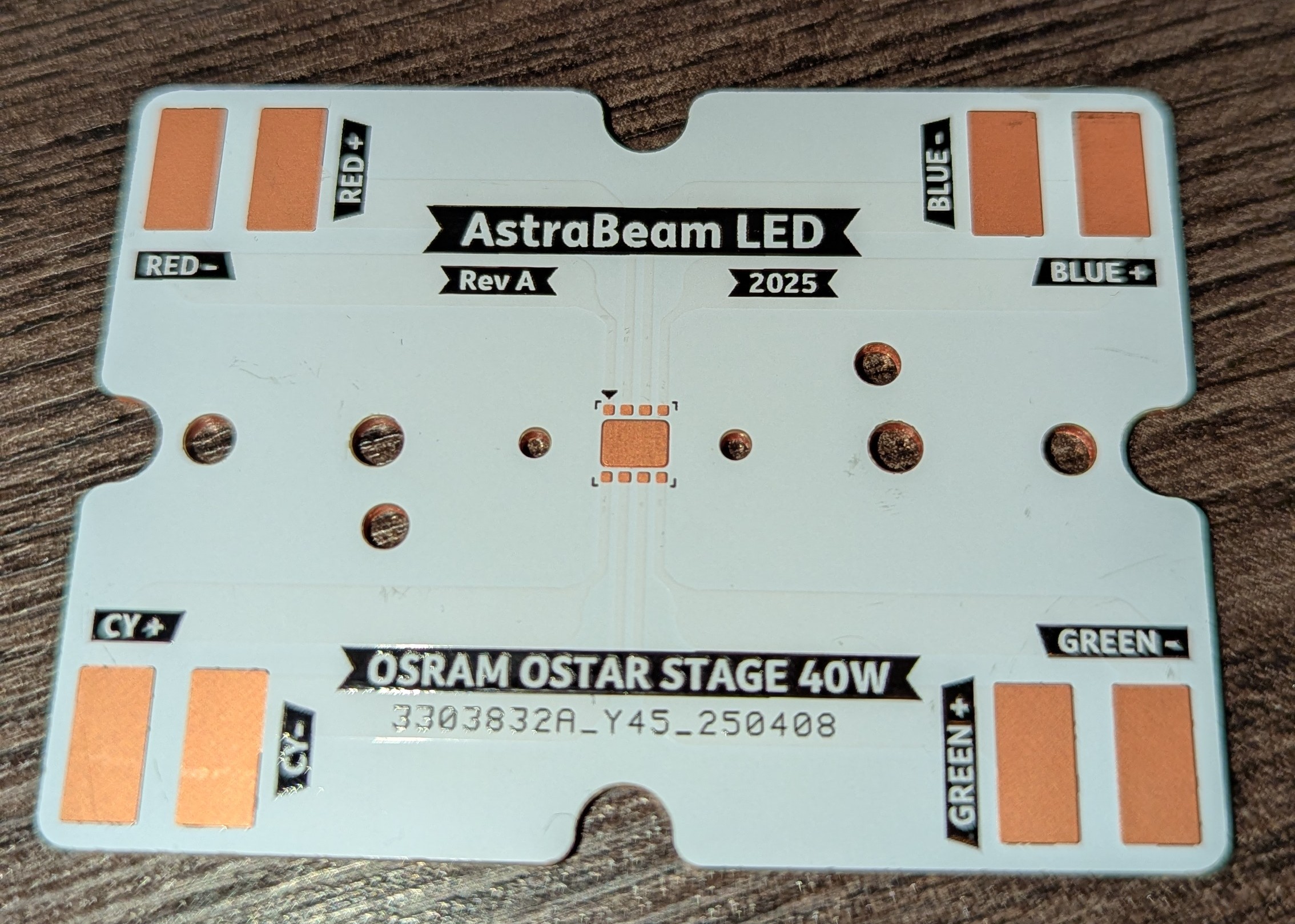
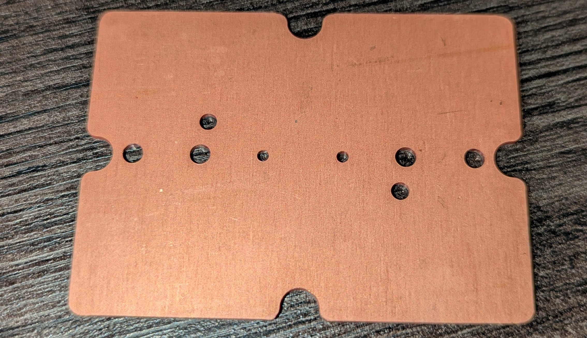
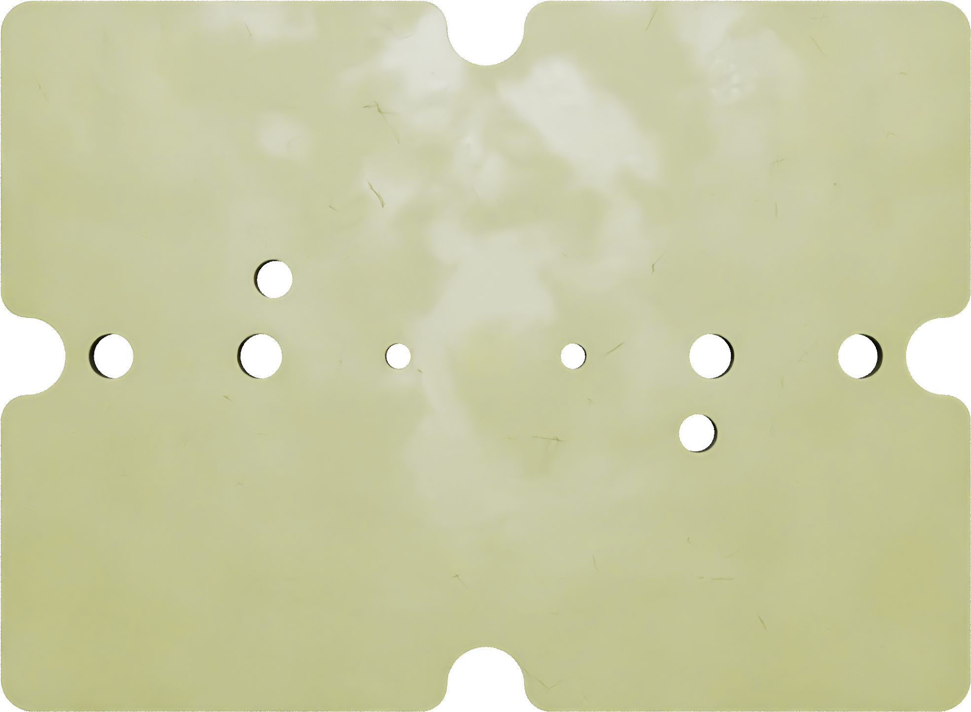
Received Product
Front
Back
Identified Issues
- Reversed Labels:
The labels for the pins were reversed (1,2,3,4 → 4,3,2,1 for both rows). This occurred because the OSRAM OSTAR LE RTDCY S2WN datasheet specifies pin numbers in the dimensional drawing as if viewed from the flipped side of the chip, rather than the standard convention used in most footprints.- This only affects the labeling. The functionality of the PCB remains intact. For example,
RED-is actuallyBLUE+, etc. - The issue has been corrected.
- This only affects the labeling. The functionality of the PCB remains intact. For example,
- Manufacturer Query:
JLCPCB was unable to determine the dimensions of the direct heatsink and inquired whether to proceed without it.
A response was sent via email, directing them to the fileAstraBeamLED-Direct_Heatsink.gbrincluded in the zip, along with an image specifying the exact dimensions.
Additional Notes
- The edges of the direct heatsink are slightly rounder than expected, with a radius of approximately 1–2 mm.
- The board is notably heavy, which is advantageous for heat dissipation.
- Soldering was performed using 138°C solder paste and a hotplate, successfully attaching an LED without any issues.
Continuous Integration and Repository Status
![]()

Table of contents
Render Top Angled
Render Top
Render Bottom
Interactive BOM
Easily check component locations by hovering over a specific component.
BOM
All components with Values, References, Sheetpath and Links to the datasheet.
KiCad Revision Inspector (KiRI)
KiCad Revision Inspector (KiRI) is a tool for comparing different versions of KiCad projects. It exports project revisions to SVG format for visual comparison using an onion skin view. This helps identify changes and errors in PCB designs. KiRI also includes a command line interface for generating viewable artifacts in any web browser.
View the PCB / Schematic in an interactive way, pan and zoom to see the details.
Dark
Light
Schematic
Dark
Monochromatic
Light
Assembly
Dark
Light
3D Step
Downloads
JLCPCB
Eurocircuits
Report
ERC
ERC Report
- Errors: 0
- Warnings: 0
- Link: HTML Report
DRC
DRC Report
- Errors: 0
- Warnings: 0
- Link: HTML Report
PCB
Board size: 75.0x55.0 mm (2.95x2.17 inches)
- This is the size of the rectangle that contains the board
- Thickness: 1.61 mm (63 mils)
- Material: FR4
- Finish: ENIG
- Layers: 2
- Copper thickness: 35 µm
Solder mask: TOP / BOTTOM
- Color: Top: #00000080 / Bottom: #0000002b
Silk screen: TOP / BOTTOM
- Color: White
Special features:
- Edge plating
Stackup:
| Name | Type | Color | Thickness [µm] | Material | Er | Loss tan |
|---|---|---|---|---|---|---|
| F.SilkS | Top Silk Screen | White | ||||
| F.Paste | Top Solder Paste | |||||
| F.Mask | Top Solder Mask | #00000080 | 10 | |||
| F.Cu | copper | 35 | ||||
| dielectric 1 | core | #8D5316ED | 1516 | FR4 | 4.4 | 0.020 |
| B.Cu | copper | 35 | ||||
| B.Mask | Bottom Solder Mask | #0000002B | 10 | |||
| B.Paste | Bottom Solder Paste | |||||
| B.SilkS | Bottom Silk Screen | White |
Important sizes
Clearance: 0.2 mm (8 mils)
Track width: 0.75 mm (30 mils)
- By design rules: 0.15 mm (6 mils)
Drill: N/A mm (N/A mils)
- Vias: N/A mm (N/A mils) [Design: 1.1 mm (43 mils)]
- Pads: N/A mm (N/A mils)
- The above values are real drill sizes, they add 0.1 mm (4 mils) to plated holes (PTH)
Via: N/A/N/A mm (N/A/N/A mils)
- By design rules: 0.3/1.0 mm (12/39 mils)
- Micro via: yes [0.2/0.1 mm (8/4 mils)]
- Buried/blind via: yes
- Total: 0 (thru: 0 buried/blind: 0 micro: 0)
Outer Annular Ring: N/A mm (N/A mils)
- By design rules: 0.1 mm (4 mils)
Eurocircuits class: 4A
- Using min drill N/A mm for an OAR of N/A mm
General stats
Components count: (SMD/THT)
- Top: 9/0 (SMD)
- Bottom: 0/0 (NONE)
Defined tracks:
- 0.35 mm (14 mils)
- 0.5 mm (20 mils)
- 0.75 mm (30 mils)
- 2.0 mm (79 mils)
- 4.0 mm (157 mils)
Used tracks:
- 0.75 mm (30 mils) (16) defined: yes
- 4.0 mm (157 mils) (24) defined: yes
Defined vias:
- 0.55/0.25 mm (22/10 mils)
- 0.7/0.3 mm (28/12 mils)
- 0.8/0.4 mm (31/16 mils)
Used vias:
Holes (excluding vias):
Oval holes:
Drill tools (including vias and computing adjusts and rounding):
Solder paste stats:
Using a paste with 87.75 % alloy, that has an specific gravity for the alloy of 7.4 g/cm³ and 1.0 g/cm³ for the flux. This paste has an specific gravity of 4.15 g/cm³.
The stencil thickness is 0.12 mm.
| Side | Pads with paste | Area [mm²] | Paste [g] |
|---|---|---|---|
| Total | 24 | 412.67 | 2.05 |
Note: this is just an approximation to the theoretical value. Margins of the solder mask and waste aren’t computed.
Credits
Amulet - Inspiration for awesome schematic and PCB
Sorry if I am forgetting someone, I used lots of references and tips from all over the place.