AstraDriver
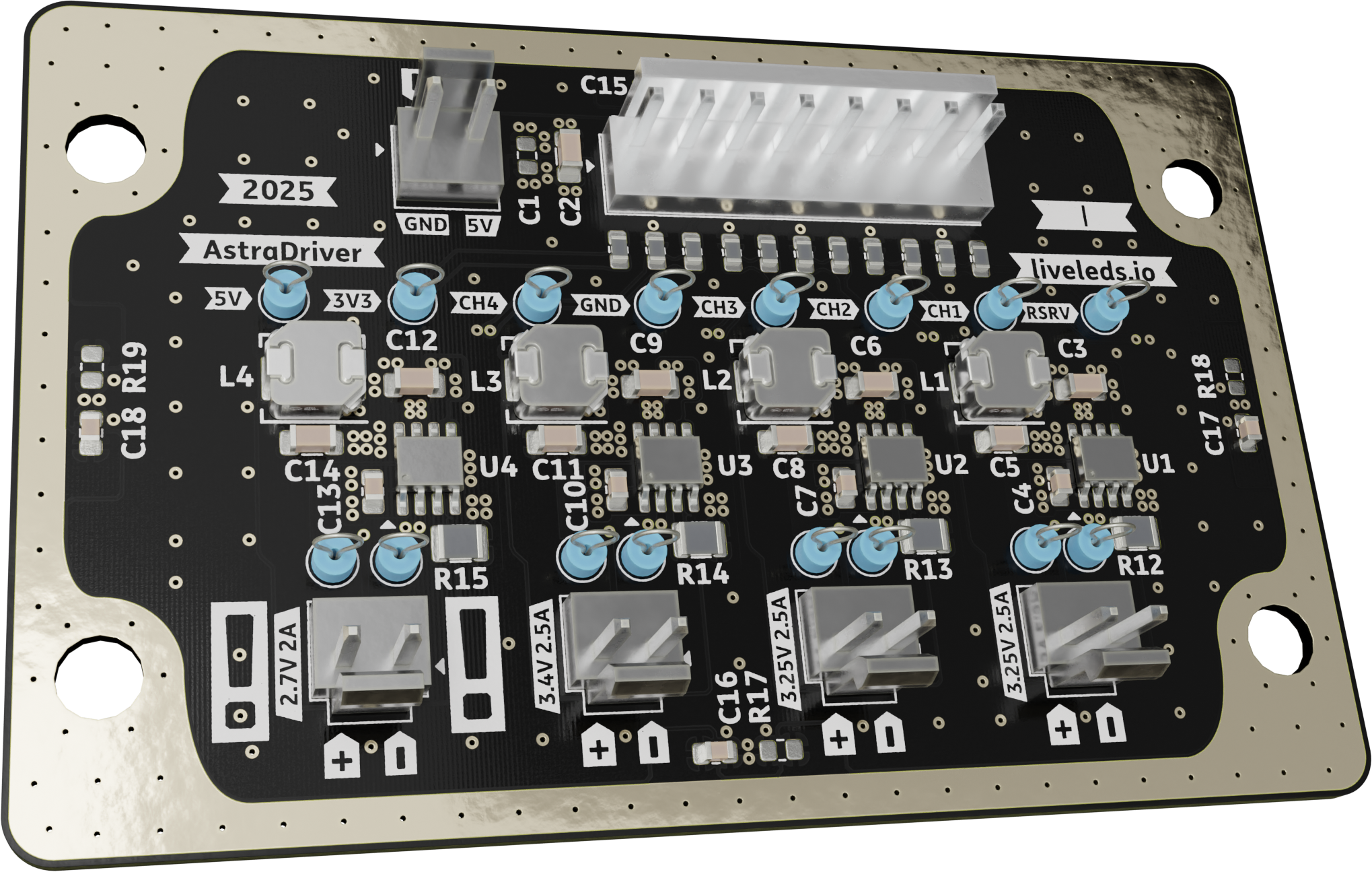
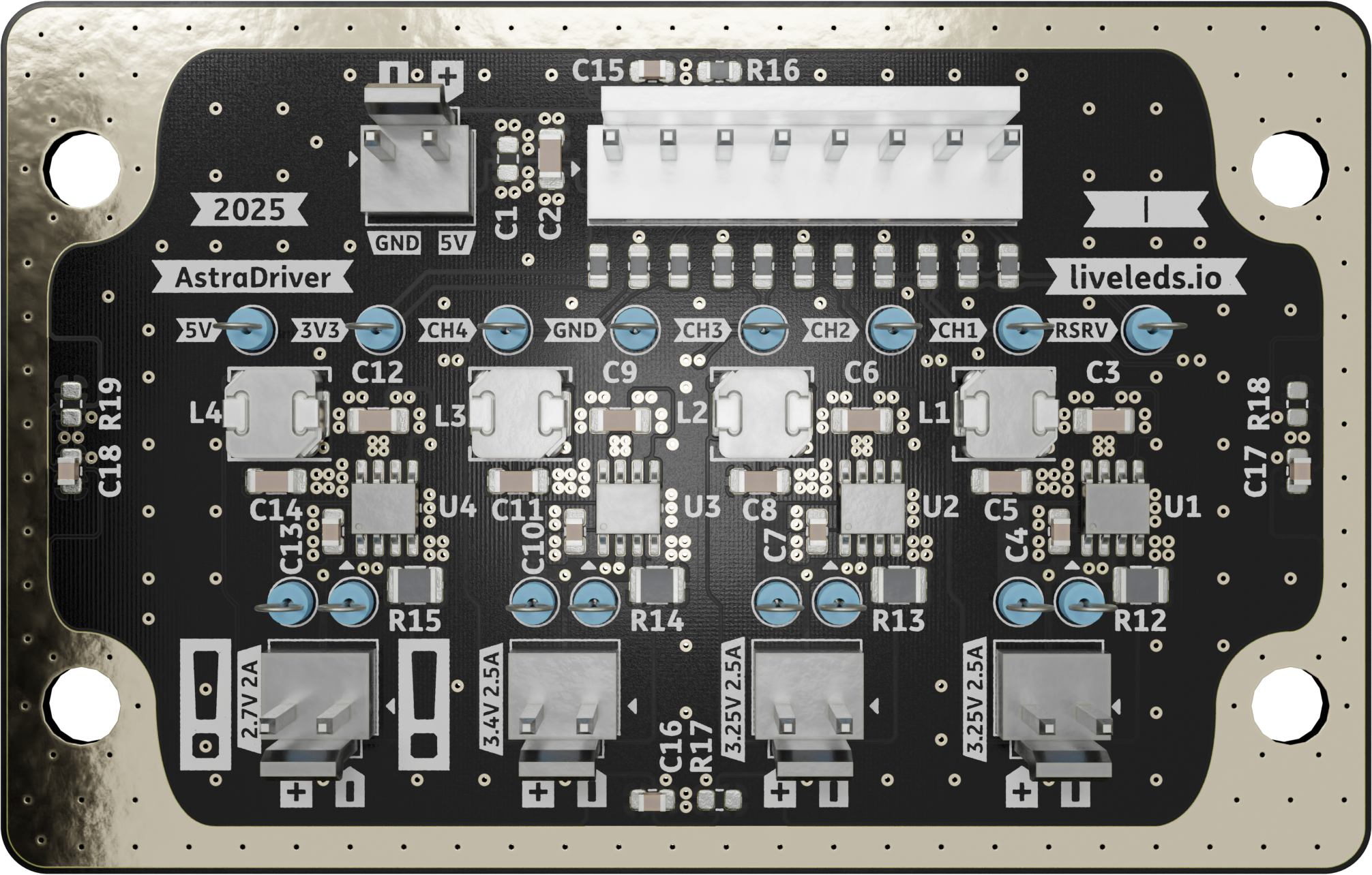
4 Channel LED Driver with PWM dimming input. LED2001PHR is the driver IC, it can support up to 4A, 3V - 18V at 850KHz switching frequency. Test plugs for each input and output. Optimized for good dimming performance. The board connects to AstraControl ESP32-based control PCB uses WiFi with an external antenna and 5Mbps RS-485. Direct copper heat-sink PCB for LED diode AstraBeamLED.
Production Details
The PCB went into production on April 9, 2025.
- Git Tag:
production-2025.04.09
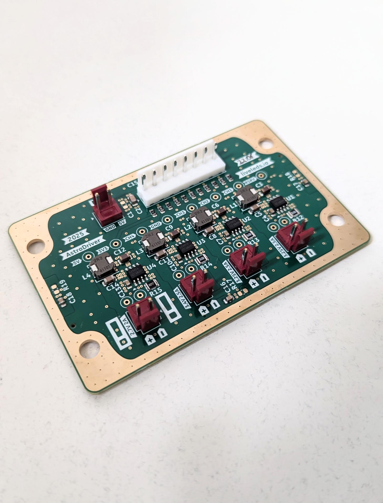
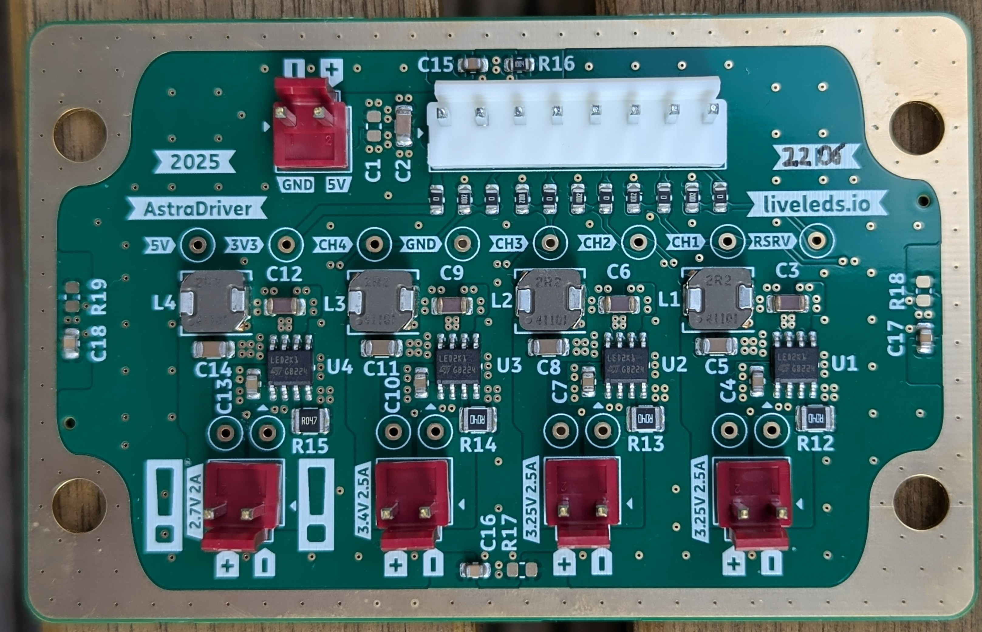
Received Product
Front
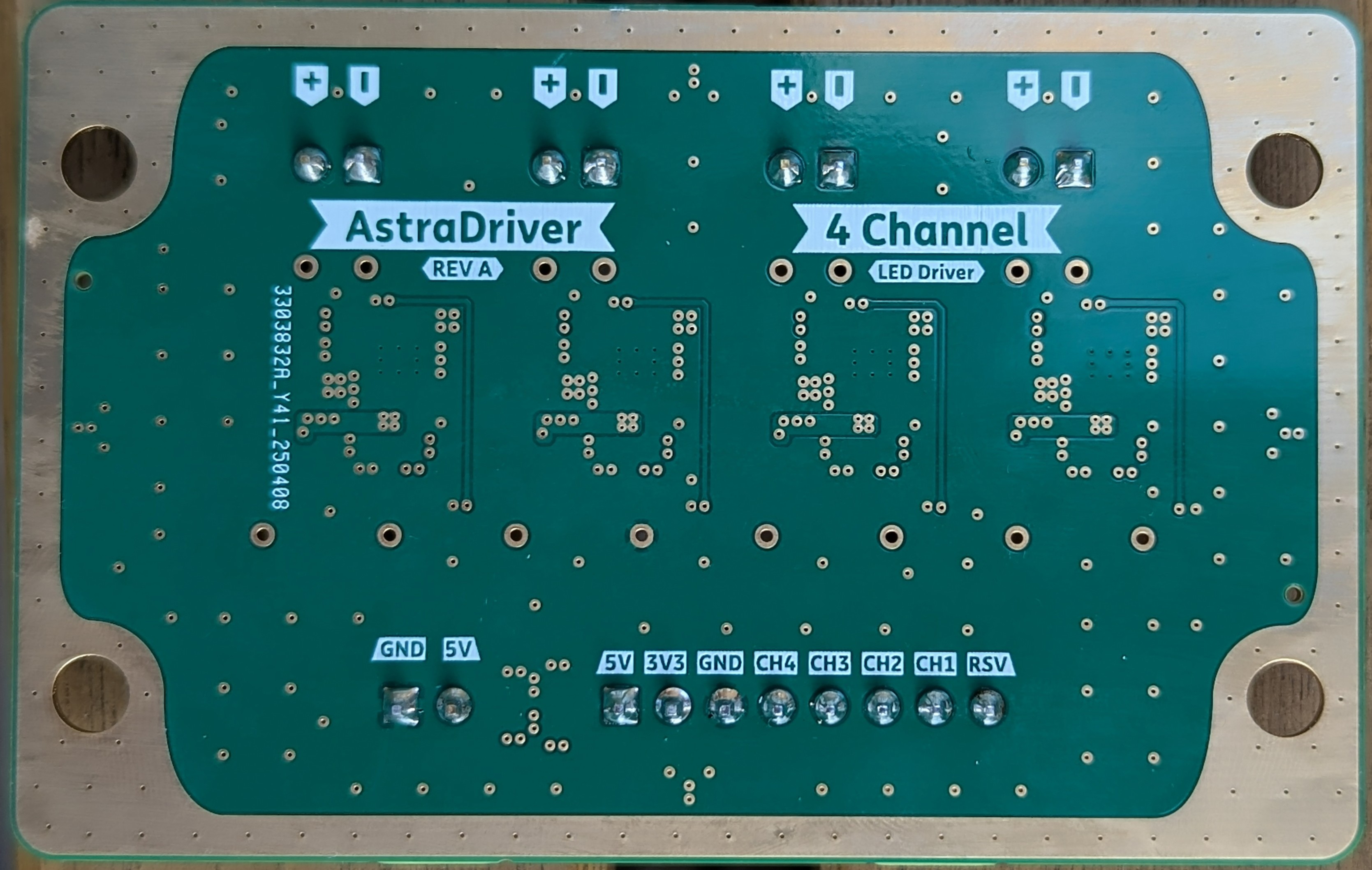
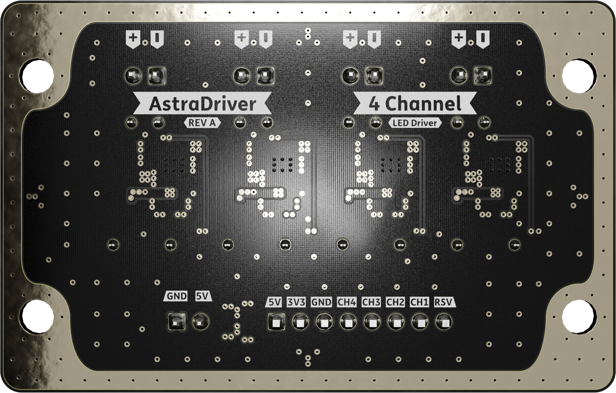
Back
Identified Issues
-
Minor Coil Whine: A very minor coil whine can be heard under full PWM operation, especially when going from 100% to 0%. It’s not very critical for my use case but I fixed the issue by adding an electrolytic 1000uF capacitor into the test plug holes (5V and GND). Something to improve in the next revision. The existing 100uF ceramic is not performing well enough.
-
Flicker at very low PWM: When testing 14 bit PWM resolution the LEDs were flickering slightly at very low values (up to 150 around %1). It’s was expected and I just limited it in software, it’s still very dim and stable at 150. A potential solution is to use an N-Channel MOSFET to control which shunt resistor (current of 2.5A or 0.5A for example) is used and select the appropriate one for very low value to have a complete 0 to 100% range. An example of such an HDR approach can be found on Youtube here (8:36): Building My Ultimate LED Flashlight: Boost Driver Circuit Episode #1 Credit to Engeneering Bo.
Additional Notes
- Overall the whole project worked without significant issues on the first revision.
- The test plug hole were very useful to add an extra capacitor, debugging PWM and checking voltages.
Continuous Integration and Repository Status
![]()

Table of contents
Render Top Angled
Render Top
Render Bottom
Schematic
Dark
Monochromatic
Light
Assembly
Dark
Light
Gerber viewer on tracespace.io
Interactive BOM
Check component locations by hovering over a specific component. The visual elements might not be precise enough for pcb review but can be very useful since it’s possible to pan and zoom. Not all BOM columns are available here, for datasheet links see BOM below.
BOM
All components with Values, References, Sheetpath and Links to the datasheet.
KiCad Revision Inspector (KiRI)
KiCad Revision Inspector (KiRI) is a tool for comparing different versions of KiCad projects. It exports project revisions to SVG format for visual comparison using an onion skin view. This helps identify changes and errors in PCB designs. KiRI also includes a command line interface for generating viewable artifacts in any web browser.
View the PCB / Schematic in an interactive way, pan and zoom to see the details.
Dark
Light
Downloads
JLCPCB
Eurocircuits
3D Step
Report
ERC
ERC Report
- Errors: 0
- Warnings: 0
- Link: HTML Report
DRC
DRC Report
- Errors: 5
- Warnings: 0
- Link: HTML Report
PCB
Board size: 102.0x65.0 mm (4.02x2.56 inches)
- This is the size of the rectangle that contains the board
- Thickness: 1.61 mm (63 mils)
- Material: FR4
- Finish: ENIG
- Layers: 4
- Copper thickness: 35 / 15 µm
Solder mask: TOP / BOTTOM
- Color: #00000080
Silk screen: TOP / BOTTOM
- Color: White
Stackup:
Impedance controlled: YES
| Name | Type | Color | Thickness [µm] | Material | Er | Loss tan |
|---|---|---|---|---|---|---|
| F.SilkS | Top Silk Screen | White | ||||
| F.Paste | Top Solder Paste | |||||
| F.Mask | Top Solder Mask | #00000080 | 10 | |||
| F.Cu | copper | 35 | ||||
| dielectric 1 | prepreg | #8D5316ED | 210 | FR4 | 4.4 | 0.020 |
| In1.Cu | copper | 15 | ||||
| dielectric 2 | core | #8D5316ED | 1065 | FR4 | 4.6 | 0.020 |
| In2.Cu | copper | 15 | ||||
| dielectric 3 | prepreg | #8D5316ED | 210 | FR4 | 4.4 | 0.020 |
| B.Cu | copper | 35 | ||||
| B.Mask | Bottom Solder Mask | #00000080 | 10 | |||
| B.Paste | Bottom Solder Paste | |||||
| B.SilkS | Bottom Silk Screen | White |
Important sizes
Clearance: 0.2 mm (8 mils)
Track width: 0.35 mm (14 mils)
- By design rules: 0.15 mm (6 mils)
Drill: 0.4 mm (16 mils)
- Vias: 0.4 mm (16 mils) [Design: 0.4 mm (16 mils)]
- Pads: 0.4 mm (16 mils)
- The above values are real drill sizes, they add 0.1 mm (4 mils) to plated holes (PTH)
Via: 0.7/0.3 mm (28/12 mils)
- By design rules: 0.3/0.3 mm (12/12 mils)
- Micro via: yes [0.2/0.1 mm (8/4 mils)]
- Buried/blind via: yes
- Total: 266 (thru: 266 buried/blind: 0 micro: 0)
Outer Annular Ring: 0.1 mm (4 mils)
- By design rules: 0.1 mm (4 mils)
Eurocircuits class: 8C
- Using min drill 0.4 mm for an OAR of 0.1 mm
General stats
Components count: (SMD/THT)
- Top: 45/23 (SMD + THT)
- Bottom: 0/0 (NONE)
Defined tracks:
- 0.3 mm (12 mils)
- 0.35 mm (14 mils)
- 0.5 mm (20 mils)
- 0.7 mm (28 mils)
- 0.9 mm (35 mils)
- 1.0 mm (39 mils)
Used tracks:
- 0.35 mm (14 mils) (57) defined: yes
- 0.7 mm (28 mils) (12) defined: yes
- 0.9 mm (35 mils) (12) defined: yes
Defined vias:
- 0.55/0.25 mm (22/10 mils)
- 0.7/0.3 mm (28/12 mils)
- 0.8/0.4 mm (31/16 mils)
Used vias:
- 0.7/0.3 mm (28/12 mils) (Count: 16, Aspect: 2.3 A) defined: yes
- 0.8/0.4 mm (31/16 mils) (Count: 250, Aspect: 2.0 A) defined: yes
Holes (excluding vias):
- 0.3 mm (12 mils) (32)
- 0.4 mm (16 mils) (102)
- 0.9 mm (35 mils) (16)
- 1.8 mm (71 mils) (18)
- 5.8 mm (228 mils) (4)
Oval holes:
Drill tools (including vias and computing adjusts and rounding):
- 0.4 mm (16 mils) (48)
- 0.5 mm (20 mils) (352)
- 1.0 mm (39 mils) (16)
- 1.9 mm (75 mils) (18)
- 5.9 mm (232 mils) (4)
Solder paste stats:
Using a paste with 87.75 % alloy, that has an specific gravity for the alloy of 7.4 g/cm³ and 1.0 g/cm³ for the flux. This paste has an specific gravity of 4.15 g/cm³.
The stencil thickness is 0.12 mm.
| Side | Pads with paste | Area [mm²] | Paste [g] |
|---|---|---|---|
| Total | 130 | 246.79 | 1.23 |
Note: this is just an approximation to the theoretical value. Margins of the solder mask and waste aren’t computed.
Know Issues
- TBD
Credits
Amulet - Inspiration for awesome schematic and PCB
tracespace view - Online Gerber Viewer